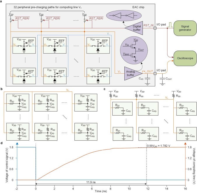
Extended Data Fig. 8. Measurement of reset time, response time and accumulating time of ACCEL and circuit modelling of reset operation.
a, Configurations of reset operation with the voltage-readout signal chains for computing lines. The voltages of computing lines are read out with an on-chip buffer for observations. The signal generator provides the control signal, which enables the reset operation when the voltage of control signal is low (ground voltage), and enables the computing process when the voltage of control signal is high (supply voltage). b, Circuit modelling of the pre-charging process of the computing line with local charging paths. c, Circuit modelling of the pre-charging process of the computing line with peripheral charging paths. d, Post-simulated timing diagram of the reset operation of computing line with local pre-charging paths.

