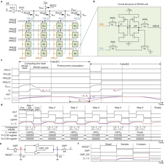
Extended Data Fig. 1. Implementation and timing diagrams of EAC circuit.
a,b, Implementation of the SRAM macro in each pixel. The SRAM unit circuit is implemented with the standard 8-transistor structure. RWL, read word-line; WWL, write word-line; RBL, read bit-line; RCL, read-column; PRCH, pre-charge. c, Timing diagram of the signals in the EAC chip during computation, which consists of four operations: SRAM reset, SRAM readout, computing line reset and photocurrent computation. Signal DOUT,i is the internal pre-charging node in the SRAM macro in ith pixel unit (1 ≤ i ≤ 1024). Signal Qi is the output of SRAM macro in ith pixel unit, determined by the stored weight wij, where 1 ≤ j ≤ Noutput labels the jth output node. The SRAM operation and reset operation of computing line can be conducted simultaneously. d, Timing diagram of the capacitance compensation process. The compensation process is performed by a binary search strategy in multiple steps to tune the load capacitance C+/C− of the computing line V+/V− to the same value. The presented 6-bit binary codes stored in the P-CCM/N-CCM registers indicate the number of the compensation photodiodes (PDC) in the P-CCM/N-CCM connected to the computing line. The variations of C+ and P-CCM/N-CCM registers illustrated in this figure correspond to the case where the number of positive/negative weights are 490/534. e, The circuit structure of the comparator. The comparator utilizes back-to-back inverters that form a latch for comparing and switches for timing controlling. f, Timing diagram of the comparator. The operation of the comparator includes three phases: reset (RESET), sample (SMP) and compare (CMP_EN).

