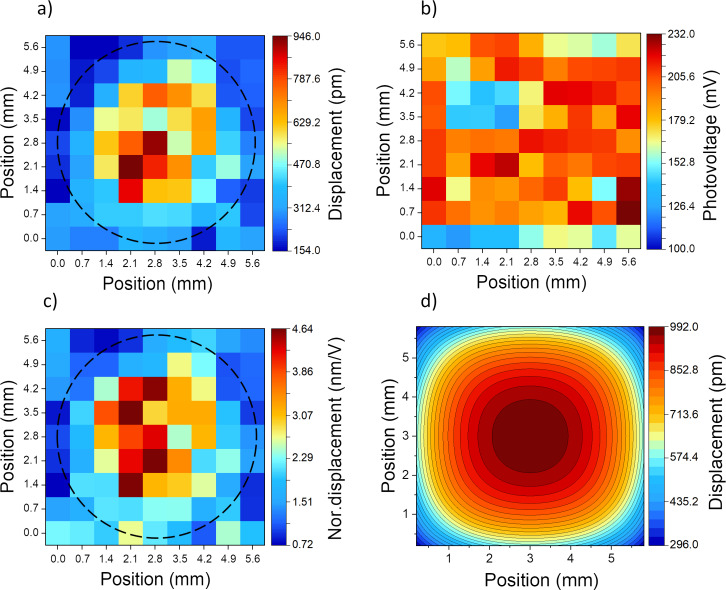
Figure 3.
Device type-I corresponding color map of (a) light-induced displacement determined at each point of a predefined grid over the surface of the device. A total of 81 points on the surface active area of 5.6 × 5.6 mm2 are mapped. The dashed black circle marks the hole etched on the backside of the silicon substrate. (b) The surface photovoltage of each measured point. (c) Displacement normalized to the corresponding photovoltage at each point. (d) Simulation results of the same sample.

