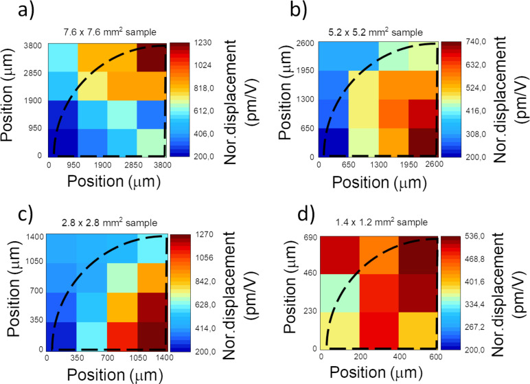
Figure 4.
Color map of the quarters of the surface area of device type-II, (a) A with dimensions of (7.6 × 7.6) mm2, (b) B with dimensions of (5.2 × 5.2) mm2, (c) C with dimensions of (2.8 × 2.8) mm2, and (d) D with dimensions of (1.4 × 1.2) mm2, where voltage-induced displacement is measured by AFM. The displacement is normalized to the corresponding voltage applied to each point.

