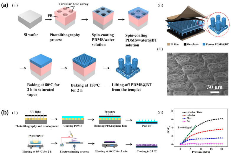
Figure 5.
(a): (i) Fabrication processes of porous micropillar dielectric layer. (ii) The structure of the capacitive pressure sensor. (iii) SEM image of the porous micropillar structure. Reproduced with permission from [29], [Ceramics International]; published by Elsevier, 2022. (b): (i) The fabrication schematics of microcylinder/electrospun fiber dual dielectric layer. (ii) Relative sensitivity comparison depending on the dielectric type. Reproduced with permission from [30], [Organic Electronics]; published by Elsevier, 2021.

