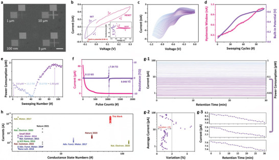
Figure 2.

a) Scanning electron microscopic image of the cross‐point structure Au/TPPS/Au OPM devices with electrode linewidth of 10 µm, 5 µm, 1 µm, and 100 nm, respectively. Bar scale: 60 µm. b) Current–voltage characteristics of the OPM device obtained by voltage sweepings from 0 to −0.1 to 0 V and from 0 to 0.3 to 0 V, respectively. Inset replots the conductance–voltage curve of the device during the same sweeping periods. c) Current–voltage characteristics of the OPM device obtained during consecutive negatively biased voltage sweepings with the stopping voltages increasing from −0.1 to −1.17 V with a ramping step of −0.01 V. Evolution of d) the memory hysteresis windows of the OPM device and built‐in potentials established across the TPPS film, as well as e) the power consumptions to read the device during the above negatively biased voltage sweepings. f) Evolution of the device currents and resistances as a function of the applied pulse numbers during the modulation with positive modulation pulse (amplitude: 0.5 V; width: 10 µs; interval: 140 µs) and a read voltage of −0.01 V. g‐1) Retention performance of 64 continuous conductance states obtained during the pulse modulation process. The device current was read using a voltage pulse with the amplitude of −0.01 V and a width of 10 µs. g‐2) summarizes the variations of the 64 state device currents recorded during the sampling period of 30 min. g‐3) displays the retention performance of 3 conductance states with middle device currents among 64 conductance states. These neighboring conductance states are inter‐distinguishable for at least 30 min. h) Comparison of device currents and number of conductances between the TPPS based OPM in this work and other memristor synapses reported in the literatures.
