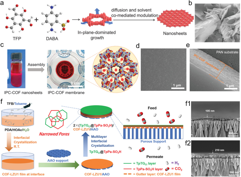
Fig. 2.
COMs preparation by layer-by-layer stacking strategy. (a) Schematic illustration of COF nanosheets; (b) SEM images of COF nanosheets; (c) schematic illustration of COMs assembly and pore structures; SEM images of COMs (d) surface and (e) cross-section [40]; (f) the fabrication of COMs COF-LZU1 with narrowed apertures using a multi-interfacial engineering strategy, and (f1, f2) SEM images of multilayer COMs with different thickness [42]. Panels reprinted with permission from: a–e, ref. [40], John Wiley and Sons; f, ref. [42], John Wiley and Sons. SEM, scanning electron microscopy.

