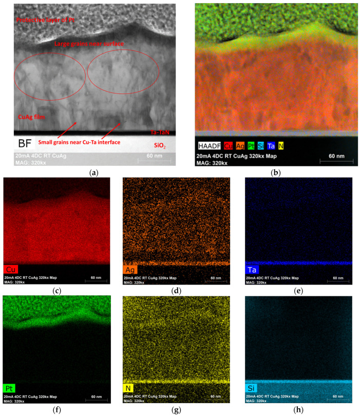
Figure 6.
(a). BF-STEM image of the cross-section of the as-deposited Cu(Ag) alloy film deposited at 4 DCs. The microstructure suggests that the surface roughness is due to the large grains of the as-deposited film. (b). The EDS overlay on the HAADF-STEM image of Cu(Ag) alloy films confirms a uniform distribution of Ag throughout the film thickness without any obvious precipitates or segregation. (c–h) EDS maps of Cu, Ag, Ta, Pt, N, and Si showing the individual distribution of these elements.

