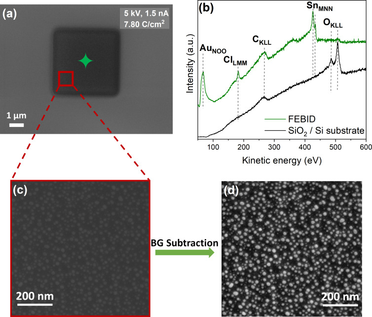
Figure 1.
(a) An SEM image of a 4 × 4 µm2 FEBID structure deposited on SiO2 from [Au(CH3)2Cl]2 with an electron dose of 7.80 C/cm2 using the electron beam parameters of 5 keV and 1.5 nA. (b) An AES plot of the SiO2 substrate prior to deposition (black line) and from the FEBID structure (green line); the green-colored star in (a) indicates the position where the spectrum was acquired. (c) Magnified image from the area within the red-colored square shown in (a). (d) The same image as shown in (c) after the background subtraction process was applied using the ImageJ program [35].

