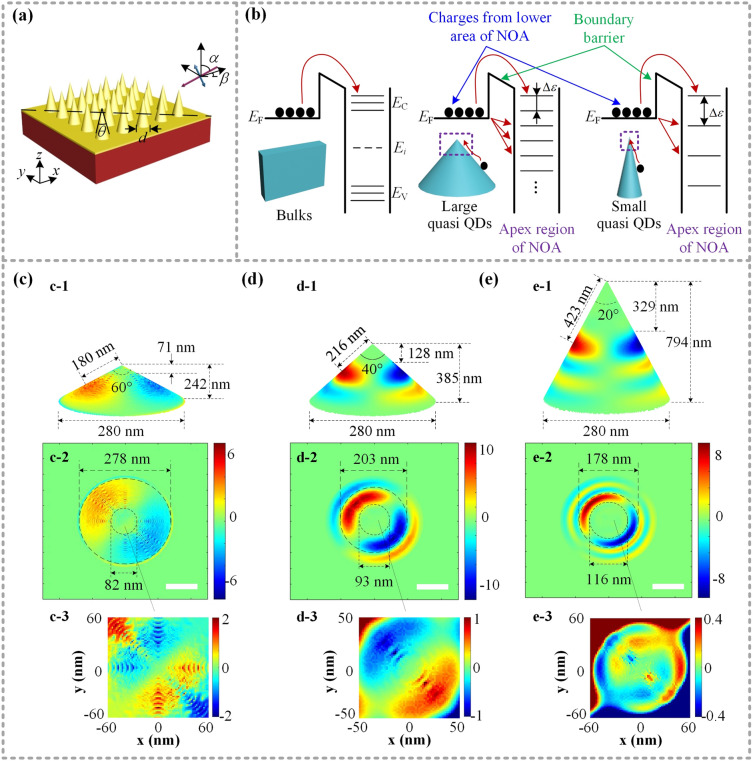
Figure 1.
Simulating the surface charge resonating distribution of metallic NOAs with different top angle θ. (a) An arrayed metal NOA illuminated by an incident beam with a central wavelength of ~ 633 nm and an initial polarization labeled by a double-sided arrow along an orientation of (α, β). (b) Energy level diagrams of typical semiconductors from bulk materials to tip-typed quasi QDs with different geometry. Typical net-charge instantaneous distribution over a single NOA with different parameters: (c) d = 280 nm, θ = 60°, (d) d = 280 nm, θ = 40°, (e) d = 280 nm, θ = 20°. The 3D simulations are exhibited by (c-1) and (d-1) and (e-1), and the main DNCS shaped by a couple of net positive charges and aggregated “free electrons” corresponding to a pixel area of 500 nm × 500 nm (scalar bar 100 nm) are shown in (c-2) and (d-2) and (e-2), respectively. Three enlarged viewings of the patterned dipole net-charge instantaneous distribution at each apex region are also presented in (c-3) to (e-3). Noting that the positive and negative signs of the right color-bars represent the positive net-charges and the aggregated “free electrons”. The adjustable upper and lower diameters of each main DNCS are roughly marked by long and short dashed circles. See details in Fig. S1 in the Supporting Information.

