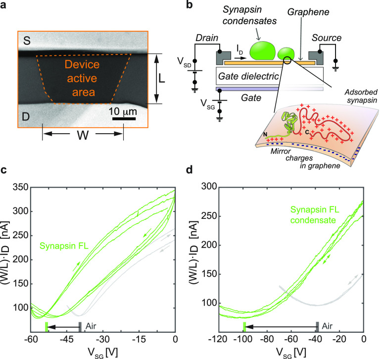
Figure 2.
Electric field induced by synapsin 1 gauged with graphene sensors. (a) An optical micrograph of one device. The estimated region for the length (L) and width (W) of the active area of Gr FET is highlighted with dashed lines. (b) Scheme of the device cross-section indicating the applied biases (voltage) and the current flow direction. The magnification illustrates the electric double layer formation at the interface-to-analyte region. (c–d) Transfer characteristics (ID(VSG)) of Gr FETs right before exposure to the analyte (gray) and while in the solution (green), respectively for (c) synapsin full length (FL) and (d) condensates of synapsin full length. The bars on the x-axis in c–d indicate the mean position of the CNPs for each case, while the arrows indicate the shift of the transfer curves upon interaction with the analytes.

