
Figure 2.
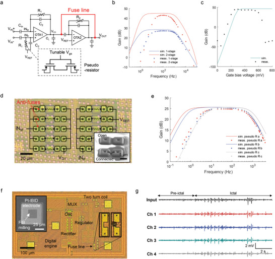
Evaluation and optimization of wired and wireless neural sensors incorporating pseudo‐resistors. a) Schematic of a two‐stage low‐noise capacitively coupled neural amplifier with a gate‐bias voltage‐controlled pseudo‐resistor (R1, R2) in a feedback loop. Each amplifier stage can be selectively tested by laser ablating the embedded fuse line (red), shorting the second stage amplifier input to output. b) Frequency responses of single‐ and two‐stage amplifiers, obtained through measurement and simulation. c) Gain of the two‐stage amplifier in response to a 100 Hz input signal as a function of the gate bias voltage (simulation and measurement). d) Photograph of an array of pseudo‐resistors and anti‐fuses, along with the state status of their connectivity to the OTA. The SEM image shows an original anti‐fuse and a connected fuse after FIB milling and Pt deposition. e) Gain and bandwidth of three versions of single‐stage amplifiers with different pairs of pseudo‐resistors, both simulated and measured. Additional details on the pseudo‐resistors are provided in Table S1 (Supporting Information). f) Wireless four‐channel EEG recording chip incorporating fuses to edit and control multiple features: pseudo‐resistor bias voltage, regulator, oscillator, and other components. The chip has dimensions of 500 µm × 800 µm. Inset in (f) shows Pt‐IBID (ion‐beam induced deposition) sensing electrodes fabricated on the wireless microchip using FIB after first milling to remove a thin aluminum oxide layer. g) Four‐channel recording of the wireless EEG microchip capturing proxy epilepsy pre‐ictal and ictal waves injected into saline. Abbreviations: sim.: simulated., meas.: measured.