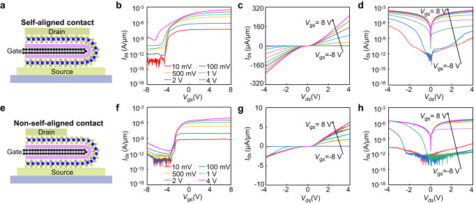
Fig. 2. Electrical properties of the devices with and without self-aligned contacts.
a Cross-sectional schematic of device with self-aligned contact. b, The drain source current–gate source voltage (Ids–Vgs) transfer characteristics of self-aligned device under various bias voltages of 10 mV (red), 100 mV (royal blue), 500 mV (yellow), 1 V (green), 2 V (slate blue) and 4 V (magenta), demonstrating an n-type behavior. c, d The linear and log plots of output characteristic of device with self-aligned contact under various gate voltages from −8 V to 8 V (2 V step). e Cross-sectional schematic of device without self-aligned contact. f Ids–Vgs transfer characteristic of device without self-aligned contact under various bias voltages of 10 mV (red), 100 mV (royal blue), 500 mV (yellow), 1 V (green), 2 V (slate blue) and 4 V (magenta). g, h The linear and log plots of output characteristic of device without self-aligned contact under various gate voltages from −8 V to 8 V (2 V step). Thickness of MoS2 is 8 layers for both devices, the channel length (Lch) of self-aligned devices is around 47 nm, and channel length of non-self-aligned devices is around 1 µm.

