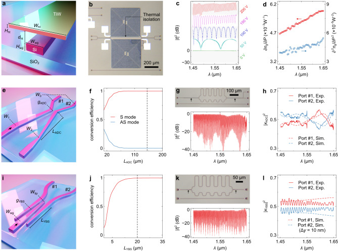
Fig. 2. Design and characterization of key components.
a 3D view of the tunable delay line. b Microscope image of the testing structure. c Measured transmittances (|t|2) at varying wavelengths (λ) when different voltages were applied. d Measured first- and second-order tuning efficiencies (∂ng/∂P, ∂2ng/∂P2). e 3D view of the adiabatic directional coupler (ADC). f Calculated conversion efficiencies of symmetric (S) and anti-symmetric (AS) modes with varying coupling lengths (LADC). g Upper panel: microscope image of the fabricated testing structure. The arrows indicate the locations of ADCs. Lower panel: Measured |t|2 at varying λ. h Calculated and measured coupling ratios (|κADC|2) of the ADC. i 3D view of the Y-branch splitter (YBS). j Calculated conversion efficiencies with varying coupling lengths (LYBS). k Upper panel: microscope image of the fabricated testing structure. The arrows indicate the locations of YBSs. Lower panel: Measured |t|2 at varying λ. l Calculated and measured coupling ratios (|κYBS|2) of the YBS. In the calculation, the central core is shifted by Δy = 10 nm.

