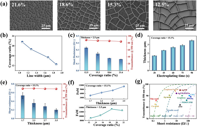
Fig. 2.
Optoelectronic characterization of Cu mesh films with different coverage ratios and thicknesses. a SEM images of Cu mesh with different coverage ratios. b Relationship between line width and coverage ratio of the Cu mesh. c Sheet resistance and optical transmittance at 550 nm of the films with different coverage ratios. d Thicknesses of the Cu mesh at different electroplating time. e Sheet resistance and optical transmittance at 550 nm of the films with different thicknesses. f FoM of the Cu mesh film with different thicknesses (up), and coverage ratios (down). g Comparison of sheet resistances and transmittances between different TCFs, which reported in the literature and this work. The dashed line indicates that FOM is equal to a specific value listed in the figure. Details about the literatures are listed in Table S3

