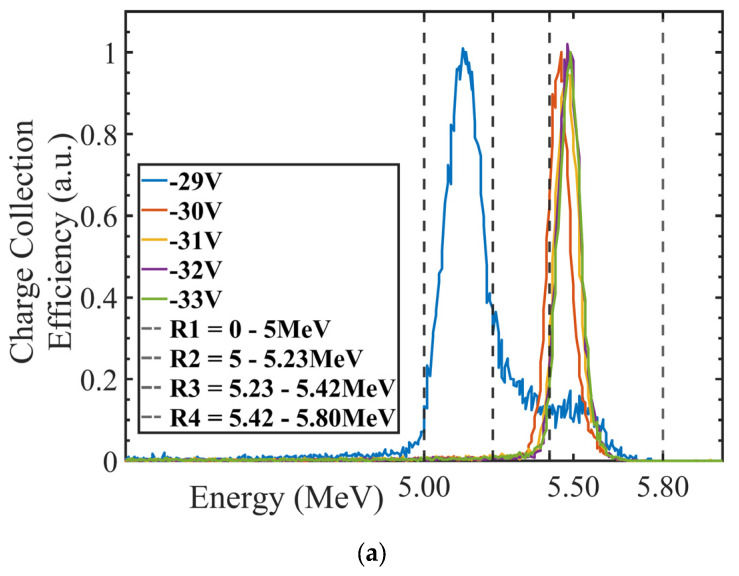
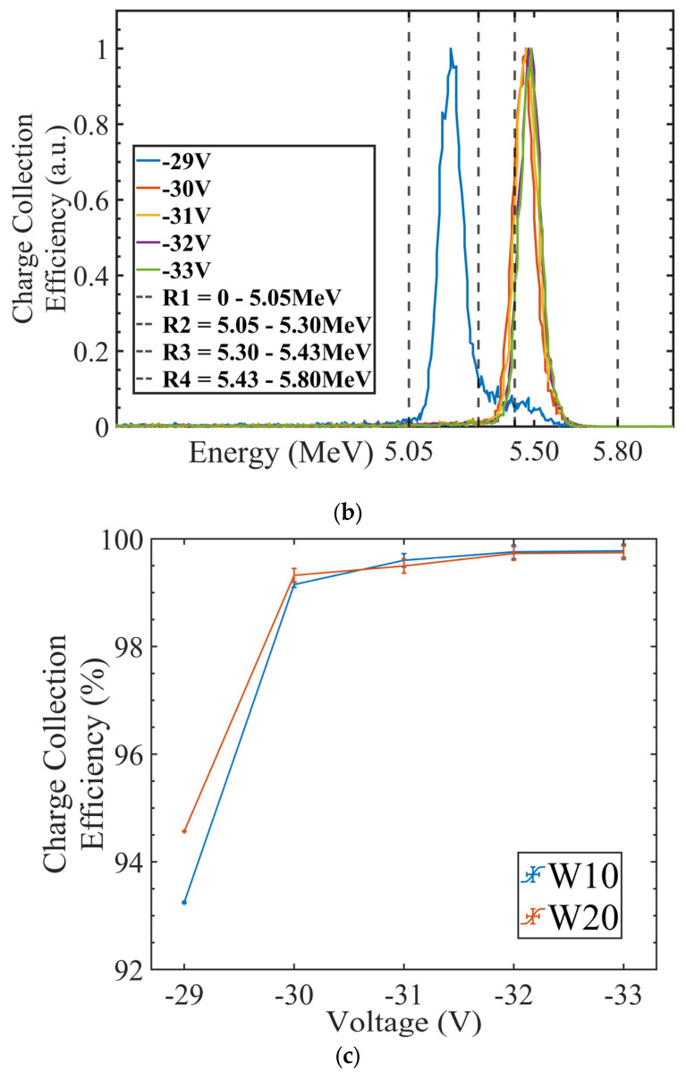
Figure 7.
(a) Wafer10 energy spectra; (b) Wafer20 energy spectra; (c) charge collection efficiency (CCE) as a function of the bias for W10 and W20 wafers with 100 and 48 micron substrate thicknesses, respectively. Error bars indicate one standard deviation from the mean value of the alpha peak energy.


