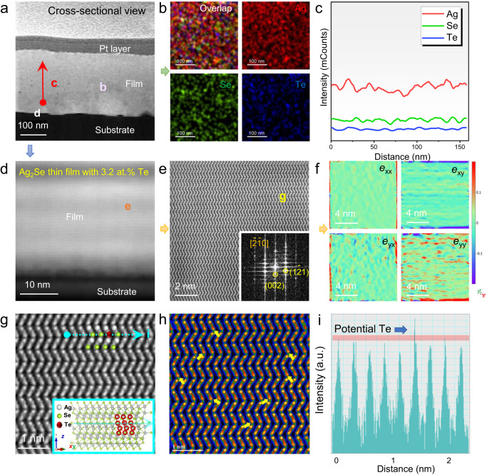
Fig. 3. Micro/nanostructural characterizations of the Ag2Se thin film with 3.2 at.% Te.
a TEM high-angle annular dark field (HAADF) image of the thin-film sample from a cross-sectional view. The sample was prepared by a focused ion beam (FIB) technique. b EDS maps for overlap and individual Ag, Se, and Te elements taken from (a). c EDS line scan taken from (a). d Spherical aberration-corrected scanning TEM (Cs-STEM) HAADF image taken from (a). e Magnified Cs-STEM HAADF image taken from (d). The inset shows the corresponding fast Fourier transform (FFT) pattern with indexed information. f Corresponding strain maps along different directions. g High-resolution Cs-STEM HAADF image taken from (e). The inset shows the crystal structure of Te-doped Ag2Se for reference. h Filtered Cs-STEM HAADF image to show the contrast difference. The arrow indicates a potential point defect of TeSe. i Line profile taken from (g) to show the potential point defect of TeSe.

