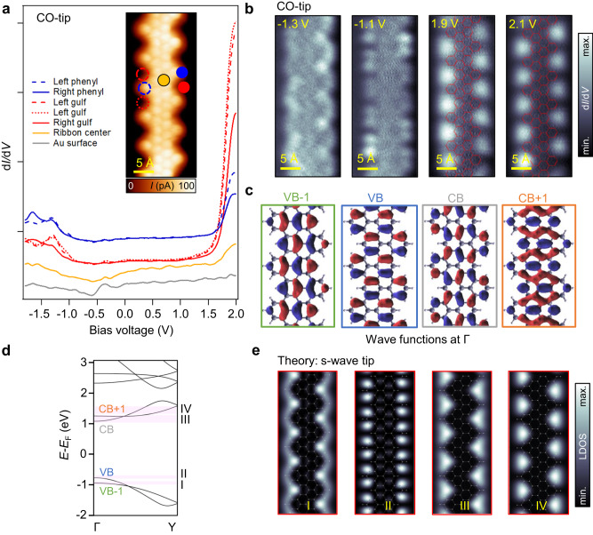
Fig. 2. Electronic properties of g-GNRs.
a dI/dV point spectra (I = 100 pA; V = 2.0 V, f = 289 Hz; Vmod (0-to-peak) = 30 mV) acquired at right (solid) and left (dashed) gulf positions (red), phenyls (blue) and at the ribbon center (orange), as well as the pristine Au(111) substrate (gray). A CO-functionalized tip is used. A wide bandgap of ≈2.8 V is observed between the onsets of the VB and CB. The inset shows a bond-resolved STM image (V = −8.3 mV) obtained by using a CO-functionalized tip in constant-height mode. b Constant-height dI/dV maps acquired near the VB [tip stabilization parameters: (V = −1.3 V, I = 40 pA) and (V = −1.1 V, I = 40 pA)] and CB [tip stabilization parameters: (V = 1.9 V, I = 50 pA) and (V = 2.1 V, I = 60 pA)] frontier orbitals reveal a very rich substructure most prominently localized at the ribbon edges (f = 289 Hz; Vmod (0-to-peak) = 40 mV). c Wave functions at the Γ point for VB, VB-1, CB, and CB + 1. d DFT electronic band structure for the g-GNR showing dispersive and braiding VBs and CBs and a semiconducting gap of 1.84 eV. e DFT-based LDOS map simulations at different energies close to the onsets of the VBs and CBs obtained at a height of z = 5 Å away from the g-GNR plane.

