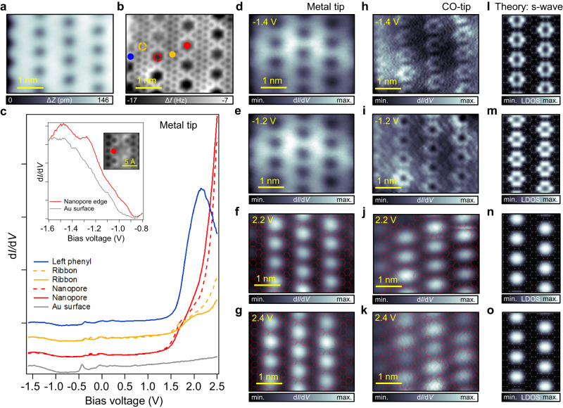
Fig. 3. Electronic properties of an NPG structure formed by the fusion of four g-GNRs.
a, b STM (V = 100 mV; I = 10 pA) and nc-AFM images of an NPG composed of four fused g-GNRs. The colored dots indicate the point spectroscopy positions. c dI/dV point spectra (I = 70 pA; V = −1.6 V; f = 954 Hz; Vmod (0-to-peak) = 20 mV) acquired at different positions of the NPG [left phenyl (blue), ribbon (orange), nanopore (red)] and Au(111) substrate (gray). Despite the weak intensity of the VB onset [see STS at the inset for a clear view of the VB peak (red) as compared to Au surface (gray) (I = 1 nA; V = −1.6 V)] compared to the prominent CB (similar to the g-GNR case), a band gap of ≈2.7 V can be extracted. d–g Constant height dI/dV maps acquired with a metal tip near the VB [tip stabilization parameters: (V = −1.4 V, I = 200 pA) and (V = −1.2 V, I = 200 pA)] and CB [tip stabilization parameters: (V = 2.2 V, I = 200 pA) and (V = 2.4 V, I = 200 pA)] frontier orbitals. The subtle VB features cannot be captured while the CB conductance features appear localized in the nanopores. h–k Constant height dI/dV maps acquired with a CO-tip (f = 353 Hz; Vmod (0-to-peak) = 40 mV) close to the onsets of the VB [tip stabilization parameters: (V = −1.4 V, I = 100 pA) and (V = −1.2 V, I = 200 pA)] and CB [tip stabilization parameters: (V = 2.2 V, I = 70 pA) and (V = 2.4 V, I = 70 pA)]. l–o Corresponding DFT LDOS map simulations as obtained using appropriate energy ranges for the VBs and CBs (see Supplementary Fig. 18).

