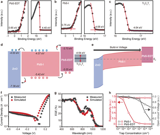
Figure 3.

Working mechanism of Ti3C2T x /PbS CQDs NIR photodiode. a–c) UPS characterization of a) PbS‐EDT, b) PbS‐I, and c) Ti3C2T x , respectively. d) Energy band diagrams of the ZnO, PbS‐I, PbS‐EDT, and Ti3C2T x before contact formation. e) Energy level alignment in the thermal‐equilibrium state for Ti3C2T x /PbS CQDs NIR photodiode. Comparison of f) dark current density and g) EQE spectra between experimental results and the theoretical model developed using Sentaurus TCAD. h) Normalized responsivity and open‐circuit voltage of PbS‐I and PbS‐EDT layers under 0.1 W cm−2 illumination with varying trap concentrations.
