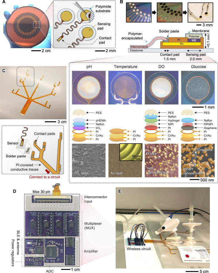
Fig. 2. System architectures of a scalable multi-sensor platform with a wireless circuit.
(A) Fabrication of an array of thin-film electrodes on a wafer; except for the sensing pad, all areas are fully covered with a polyimide (PI), enabling individual transfer to a different substrate. (B) Photos of electrodes before and after electrochemical deposition of active materials (top) and a schematic illustration and photos of the detailed structural design of four sensors (bottom); there are pH, temperature, DO, and glucose sensors with different designs of embedded layers for functionalization. Bottom scanning electron microscopy images show the top surface of each sensor. (C) Photos of a fabricated thin-film interconnect layer to integrate four sensors (top) and an exploded drawing of the strategy showing the attachment of each sensor to the interconnector (bottom). (D) Top view image of a completed wireless circuit system incorporating multiple functional components [e.g., multiplexer for each sensor, analog-to-digital converter (ADC), Bluetooth low energy (BLE), and antenna] for direct integration with different types of bioreactors. (E) Photo of a bioreactor using a single-use cell bag that has a wireless circuit for data acquisition.

