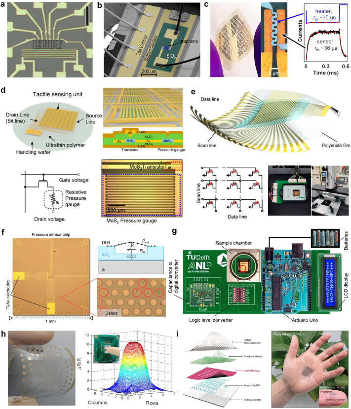
Fig. 15.
Temperature, pressure, and strain sensors based on 2D materials. a Optical microscope image of single-material graphene thermocouples showing the measurement configuration. Reproduced with permission [225]. Copyright (2020), Wiley–VCH. b Scanning electron microscopy image of the on-chip integrated graphene thermometer. Reproduced with permission [227]. Copyright (2023), American Chemical Society. c Optical images of the flexible substrate with MoS2 temperature sensor arrays, and sensor response upon pulsed actuation with the heater. Reproduced with permission [228]. Copyright (2022), American Chemical Society. d Schematic illustration of the fully integrated active-matrix MoS2 tactile sensor array, circuit diagram, and optical micrograph of thin-film transistor enabled single pressure gauge unit. Reproduced with permission [229]. Copyright (2019), American Chemical Society. e Active-matrix pressure sensors based on air-dielectric mos2 transistors for wide detection ranges from footsteps to cellular motions. Reproduced with permission [230]. Copyright (2020), American Chemical Society. f Optical image of the sensor chip based on double-layer graphene/PMMA membranes and Ti/Au electrodes. g Readout circuitry PCB board and the red circle indicates the pressure sensor chip. Reproduced with permission [231]. Copyright (2020), Nature Publishing Group. h Optical image of strain sensors with an 8 × 8 device array and measurement of the electric response on applying finger touching. Reproduced with permission [235]. Copyright (2015), American Chemical Society. i Schematic illustration of the structure of pressure sensor arrays based on the photo-reticulated strain localization films, and optical photographs of sensor arrays attached on palm. Reproduced with permission [236]. Copyright (2023), Nature Publishing Group

