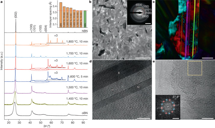
Fig. 1. XRD patterns and microstructure of the bulk ceramics prepared through SPS.
a, XRD patterns of bulk ceramics prepared under different SPS conditions. In some patterns, details of the circled regions are shown with intensity magnified by a factor of 3. Inset shows the interlayer spacing of prepared ceramics as a function of synthesis condition. b, Microstructure of the ceramic sintered at 1,600 °C for 5 min, showing randomly oriented nanoplates. Inset shows the corresponding SAED pattern, with hBN diffraction signals labelled. Extra diffraction halos and spots are present that do not belong to hBN. c, Differential phase contrast image of an edge-on nanoplate showing parallel nanoslices with different colours, indicating a laminated structure of BN nanoplates with parallel-stacked multiple BN nanoslices. d, HAADF-STEM image showing alternating regions of striped (I, III and V) and atomic (II and IV) resolution, evidencing differently twisted BN nanoslices in a laminated nanoplate. e, TEM image showing a moiré superlattice. The inset shows a fast Fourier transform pattern from the box region, where the rotational angle between two sets of diffraction spots (marked in red and blue, respectively) is 27.8°. Scale bars, 400 nm (b), 50 nm (c), 4 nm (d,e), 5 nm−1 (b,e, inset).

