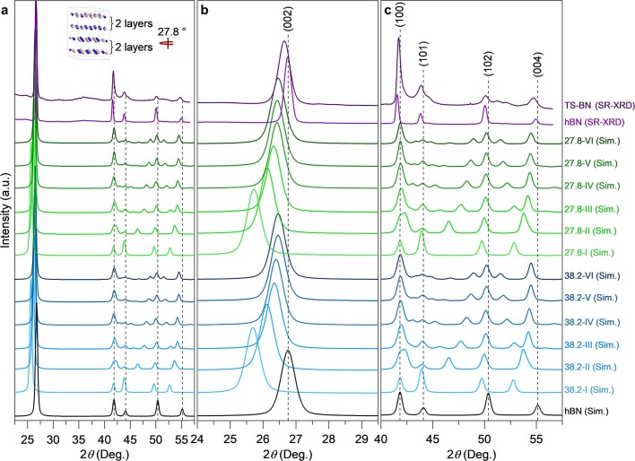
Extended Data Fig. 5. Simulated XRD patterns of hypothetical twist-stacked BN structures.
a, Full patterns. Inset shows one twist-stacked structure, constructed by two-layer-thickness BN nanoslices stacked at a twist angle of 27.8°. b and c, Expanded patterns for details. Blue and green curves: crystal structures constructed by stacking nanoslices at a fixed twist angle (38.2°or 27.8°), where each nanoslice consists of 1 to 6 atomic layers (labeled as I through VI on the right-hand side, with twisting angle as prefix). Black curve: simulated XRD pattern of hBN structure. Purple curves: synchrotron radiation XRD (SR-XRD) patterns of as-prepared TS-BN and hBN ceramics measured at room temperature. The selected wavelength of X-ray for simulation was 1.54 Å. The van der Waals interaction between layers as well as interlayer spacings of the structures are corrected according to the difference between the simulated and measured interlayer spacings of hBN. Compared with hBN, the (002) diffraction peaks of twist-stacked structures shift to the left, indicating expanded interlayer spacings. Moreover, the twist-stacked structures possess additional diffraction peaks located between (100) and (004) diffraction lines of hBN. With increasing nanoslice thickness, these new diffraction peaks gradually approach to the (101) and (102) diffraction peaks of hBN. The result shows that the introduction of twist-stacked structures can account for the extra features in XRD patterns observed experimentally. The peak positions, Miller indices, and relative intensities of simulated diffraction peaks of hypothetical crystal structures are listed in Supplementary Table 1.

