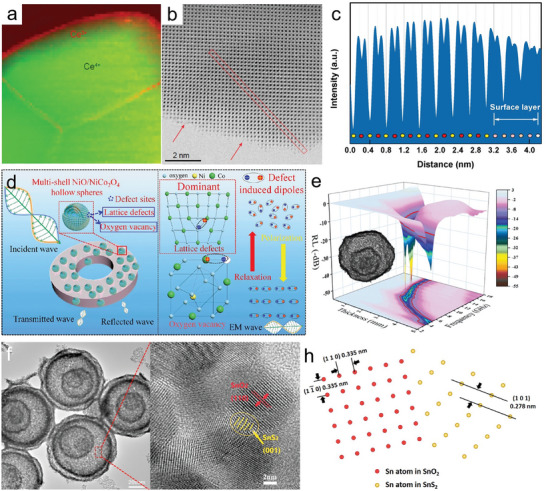
Figure 8.

a) EELS mapping of Ce3+ and Ce4+, showing their distribution in the crystals (green: Ce4+ and red: Ce3+). b) Spherical aberration‐corrected STEM image of a subunit of 3S‐CFHoMS (the single crystal surface, with red arrows indicating the atom steps). c) Corresponding line profile of the red area in (b) with the direction from the upper left to the bottom right.[ 96 ] Reproduced with permission. Copyright 2020, Oxford University Press. d) EM wave absorption mechanism of defects in NiO/NiCo2O4 HoMS. e) Reflection loss value verse frequency and corresponding 2D plots with different thicknesses for NiO/NiCo2O4 HoMS. Reproduced with permission. Copyright 2021, Wiley‐VCH. f) TEM image of SnS2/SnO2 HoMSs and corresponding enlarged HRTEM images. g) Atom model at the interface between SnS2 and SnO2 in atomic scale.[ 97 ] Reproduced with permission. Copyright 2020, Wiley‐VCH.
