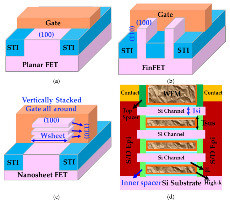
Figure 1.
Schematics of (a) a planar device, (b) a FinFET, (c) a vertically stacked bulk GAA NS FET, and (d) a cut of bulk GAA NS FET across the source-drain region where the key components marked with blue text are: surface orientations of Si channels in a planar FET, a FinFET, and a bulk NS FET, respectively, the thickness of the NS Si channels (Tsi), the width of the NS Si channels (Wsheet), GAA architecture, and inner spacers for gate and source/drain isolation physically.

