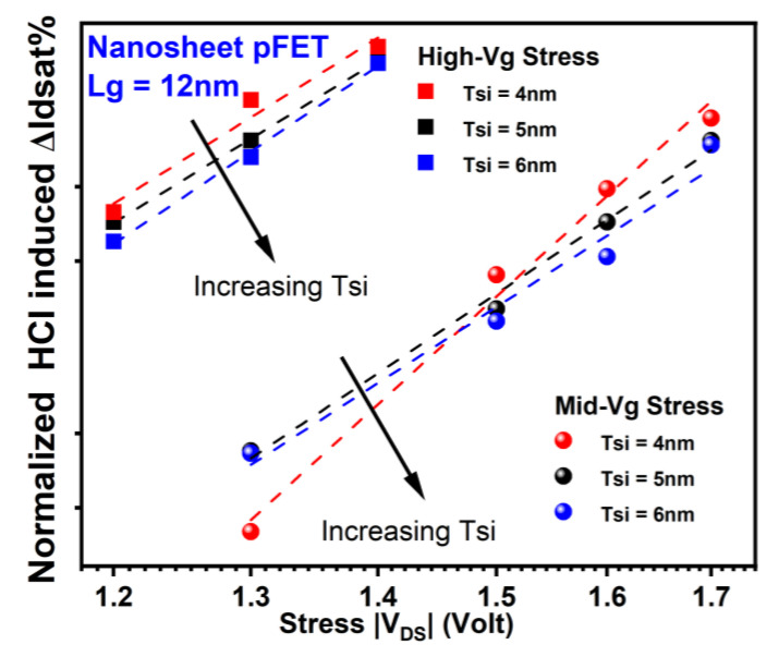
Figure 12.
HCD as a function of stress drain voltage in GAA pFETs for different Tsi. Each data point is the mean value of more than seven devices stressed at the same condition. Enhanced HCI damage at thinner Tsi can be attributed to more severe corner field crowding effect at scaled diameters of the curved region [18,21,22]. Stress gate voltage is equivalent or close to stress drain voltage under high-Vg stress conditions. Stress gate voltage is roughly between 0.5× and 0.7× of stress drain voltage for Mid-Vg stress conditions.

