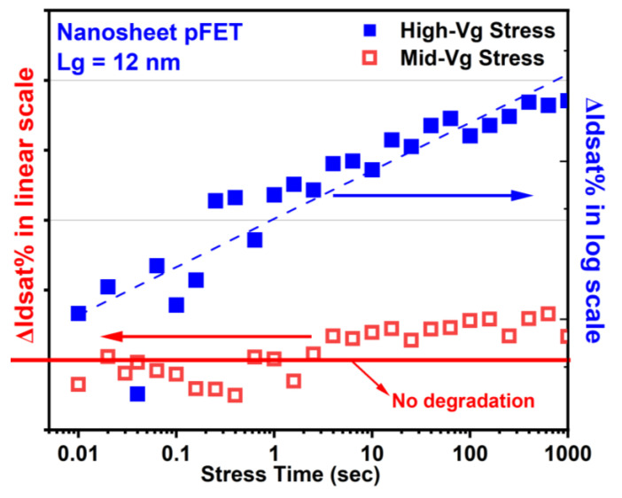
Figure 17.
Typical HCD as a function of stress time in GAA NS pFETs with Lg = 12 nm under high-Vg and Mig-Vg HC stress conditions. High-Vg HCD in NS pFETs follows power law time dependence [18]. Mid-Vg HCD in NS pFETs at low stress drain voltages no longer follows power law time dependence and is dominated by electron trapping for a short stress time, causing a current increase in contrast to the current decrease resultant from interface state generation hole trapping [62,63]. Stress gate voltage is equivalent or close to stress drain voltage under high-Vg stress conditions. Stress gate voltage is roughly between 0.5× and 0.7× of stress drain voltage under Mid-Vg stress conditions.

