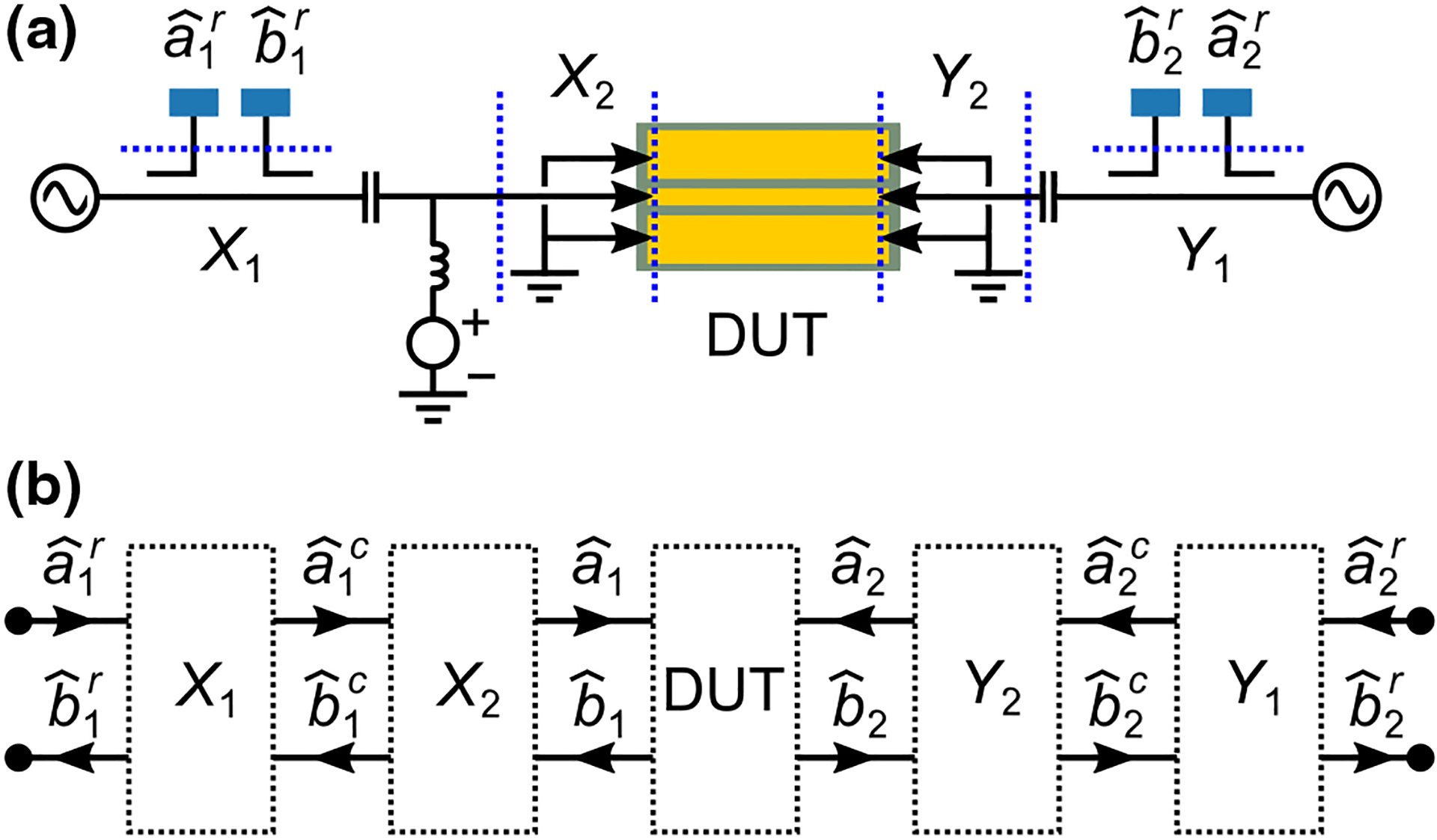
FIG. 3.

Error model. (a) Physical location of the reference planes. The raw wave parameters, and , are measured by the detectors of the LSNA. The wave parameters at the coaxial plane, and are measured at the ends of the coaxial connectors that attach to the wafer probes. The wave parameters of the device under test (DUT), and , are measured at the wafer probe tips. (b) Schematic representation of the error model relating the wave parameters at the different reference planes. The error model has 16 parameters defined independently at each frequency point: and , are all complex-valued matrices.
