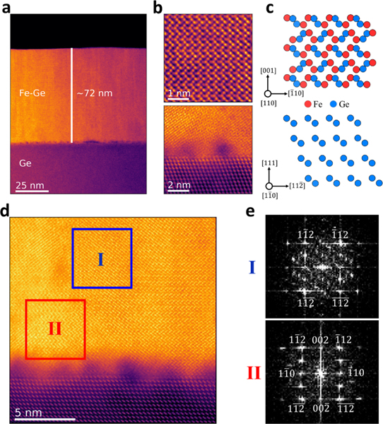
FIG. 2.
(a) HAADF image showing Ge substrate and FeGe film. (b) Atomic resolution HAADF images showing the B20 phase (top) and Ge-FeGe interface (bottom). (c) Atomic model of B20-phase (top) and Ge with crystal orientation consistent with their respective HAADF images in (b). (d) Regions I (blue) and II (red) highlight two regions with different orientations of FeGe film. (e) Fast Fourier transform (FFT) patterns of the regions I (top) and II (bottom).

