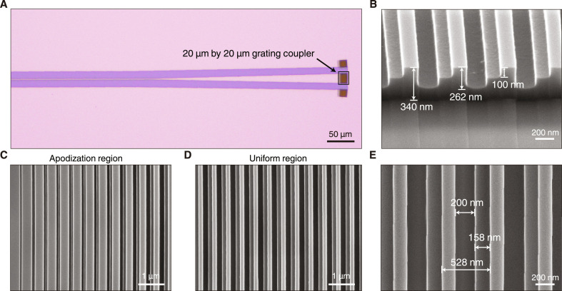
Fig. 3. Sample fabrication.
(A) Optical microscope image of the grating coupler composed of the waveguide, tapered waveguide, and grating coupler with a footprint of 20 μm by 20 μm. (B) Scanning electron microscope image of the fabricated grating coupler from a side view. (C to E) Scanning electron microscope images of (C) the apodization region and (D and E) the uniform regions of the grating coupler.

