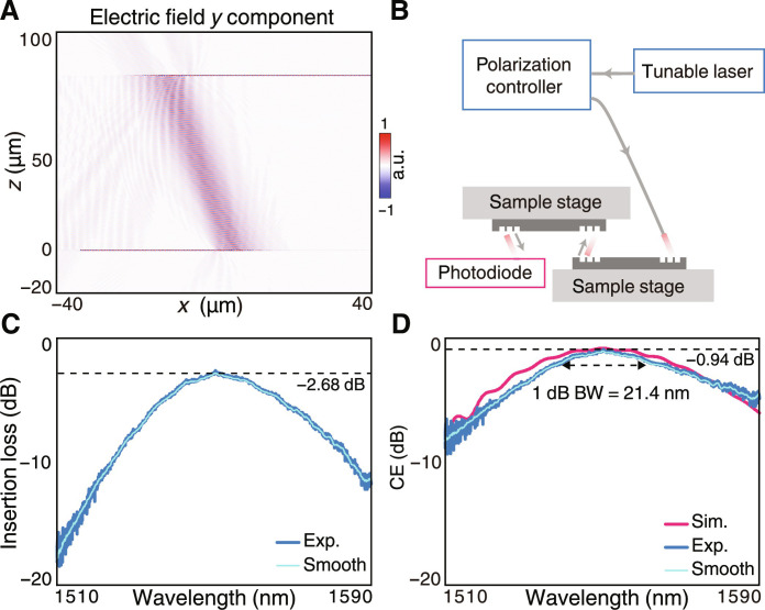
Fig. 5. Characterization of interlay CE.
(A) The electrical field distribution at 1550 nm of a pair of interlay grating couplers worked as optical via that vertically connects two photonic chips. (B) Schematic of measurement setup for interlay optical interconnect. (C) The measured insertion loss of the entire optical link that contains four unidirectional grating couplers and waveguides in a total length of 10 mm, showing a minimal loss of −2.68 dB. (D) The measured interlay CE with the peak CE of −0.94 dB and the 1-dB bandwidth of 21.4 nm.

