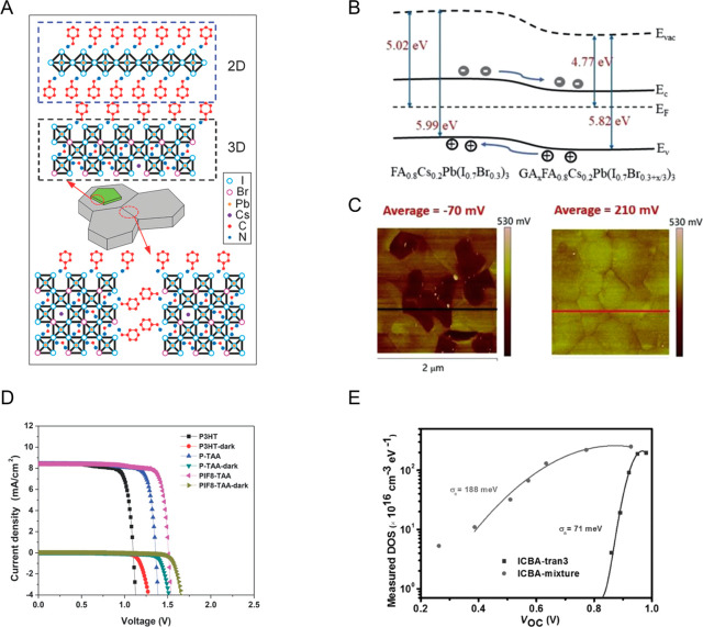
Figure 3.
(A) Schematic diagram of 2D/3D interface at the 3D perovskite surface and grain boundaries. Reprinted with permission from ref (72). Copyright 2017 Wiley-VCH. (B) Schematic energy diagram of 3D perovskite treated with guanidinium bromide(GABr). (C) Kelvin probe force microscopy (KPFM)-measured surface potential of 3D perovskite film treated without (left) and with GABr (right). (B and C) Reprinted with permission from ref (74). Copyright 2019 Elsevier. (D) J–V curves of MAPbBr3 PSCs with different HTLs. Reprinted from ref (75). Copyright 2014 Wiley-VCH. (E) Measured density of states (DOS) of perovskite devices with ICBA-mixture or ICBA-tran3 extracted from impedance results. Reprinted from ref (76). Copyright 2017 Wiley-VCH.

