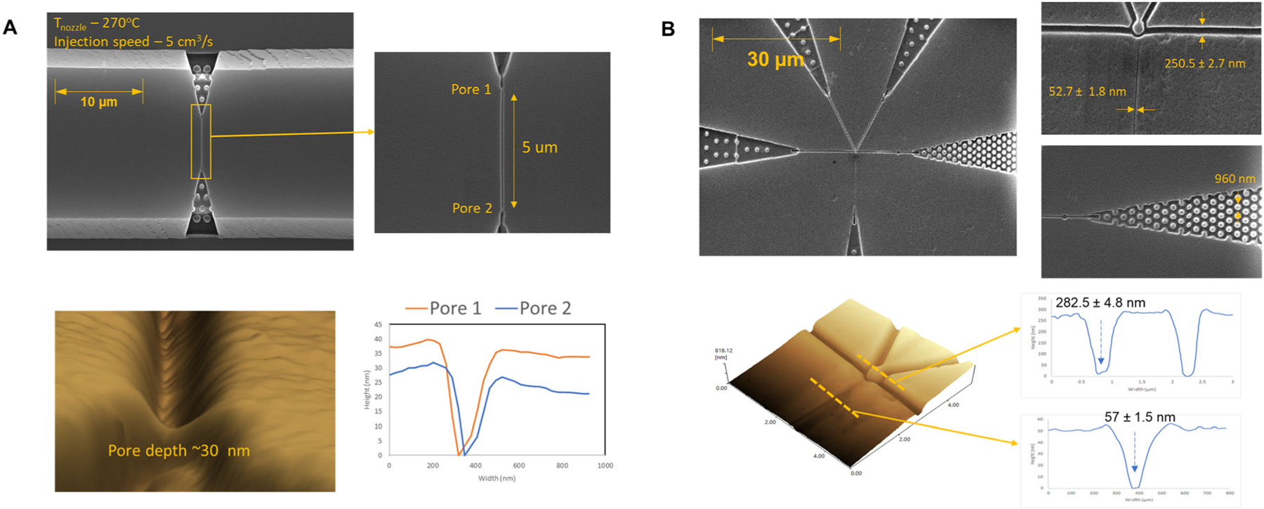
Fig. 2.

Production of nanofluidic structures by injection molding with COP from MD700 resin molds. (A) Top: Scanning electron microscopy (SEM) images of dual in-plane nanopore time-of-flight (ToF) sensor that consists of dual in-plane nanopores flanked into both ends of a nanochannel. Bottom: Atomic force microscopy (AFM) image of an in-plane nanopore (from resin mold 2, see Fig. 1B) with a ultrasharp AFM tip and cross-sectional profiles of both in-plane nanopores. (B) Top: SEM images of the nanofluidic structure used for selective binding of a single RNA molecule. The structure consists of a solid phase bioreactor located in the center of the image, four input/output nanochannels, and a nanochannel for capturing the reaction products from the solid phase reactor. The input/output channels also contain in-plane sensing pores and entropic trap. Bottom: AFM image near the solid phase bioreactor and cross sectional profiles of the nanochannels at two different locations. Both input/output channels were ∼280 nm in width and depth.
