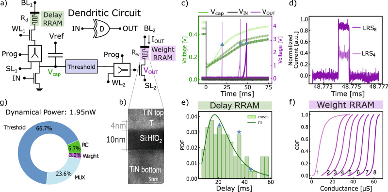
Fig. 2. Dendritic circuit, the building block of the DenRAM architecture.
a Detailed schematics of the Dendritic circuit, featuring the Delay and Weight RRAM devices, a Capacitor, dedicated multiplexers (MUX) for switching between programming and reading operations, and a Threshold circuit. b Scanning Electron-Microscopy image of a HfxO-based RRAM device used in the Dendritic circuit. c Measurement of the Dendritic Circuit, featuring the voltage on the Capacitor (Vcap), and output (VOUT). The input voltage pulse IN is applied at t = 0 s and is not shown in the plot. d Probability Distribution Function (PDF) of the delay measurements, with a log-normal distribution fitting curve. e Effect of the Weight RRAM on the output current IOUT measured from the Dendritic Circuit. Higher values of conductance (conductance G8 larger than G4, referencing the conductance levels in f) increase the output current IOUT. f Cumulative Distribution Function (CDF) of the Weight RRAM conductance values measured in a 16kb array, in different resistive states. g Breakdown of the dynamic power consumption of the dendritic circuit, showing the contributions from all the components in part (a). The highest power is attributed to the Threshold block responsible for the 66.7% of the total consumption.

