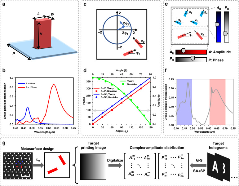
Fig. 2. Design of c-silicon nanopillars of the MCP metasurface and continuously tuning of amplitude and phase.
a Schematic diagram of a single c-silicon nanopillar (red) with width W, length L, and height H standing on the fused SiO2 substrate (blue). b Simulation results of a periodic single unit with L = 80 nm (blue line) and 170 nm (red line), respectively. The width, height, and period are fixed (W = 40 nm, H = 600 nm, P = 400 nm). The cross-polarized transmission, i.e., RCP/LCP conversion, is normalized. c The diagram of a coherent pixel is in the lower right corner, and the rotation angles of these two nanopillars are φ1 and φ2. The upper left diagram shows the transmission field in vector space, where these two vectors correspond to the functions of two nanopillars respectively. d The simulation results of a single coherent pixel. The green line and dots represent the results of amplitude manipulation. The blue and red show the results of phase adjustment. The period P is 550 nm. e Schematic of a typical MCP for arbitrary complex-amplitude tuning of transmitted waves. Each unit cell consists of six c-silicon nanopillars with rotation angles from φ1 to φ4, relative to the horizontal axis. The period P is 800 nm. f The simulated cross-polarized transmission of the structure which is shown in Fig. 2e, and the rotation angle of six nanopillars is 0°. g Flow chart of designing MCP metasurface. The left side is a scanning electron microscopy (SEM) image of a partial region of the fabricated c-silicon metasurface, and the colors we add (red and blue) correspond to the working wavelengths. The scale bar of this SEM image is 800 nm. SA sample array, SP spiral phase, G–S optimized G–S algorithm

