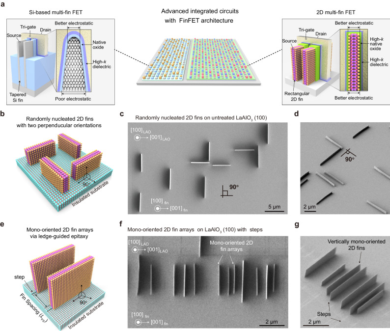
Fig. 1. Ledge-guided epitaxy of mono-oriented vertical 2D fin arrays for 2D multi-fin field-effect transistors (FETs).
a Schematic illustration for 2D multi-fin FETs potentially applied in advanced integrated circuits. b–d Schematic (b) and corresponding scanning electron microscopy (SEM) images of 2D Bi2O2Se fins with two perpendicular orientations on pristine LaAlO3 (100) surface, including top view (c) and tilted view (d). e–g Schematic (e) and corresponding SEM images of ledge-guided epitaxial mono-oriented 2D Bi2O2Se fins on pre-treated LaAlO3 (100) surface, including top view (f) and tilted view (g).

