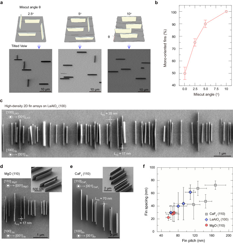
Fig. 3. Guided-growth of mono-oriented high-density 2D fin arrays for 2D multi-fin FETs with the assistance of steps.
a Schematic and SEM images showing the effect of the step density on the orientation of 2D Bi2O2Se fin arrays. b Statistic for mono-oriented fin percentage of 2D Bi2O2Se fin arrays growth with miscut angle of the epitaxial substrate. Error bars indicate standard deviations of mono-oriented fin percentage for different miscut angle. c–e SEM images of high-density 2D Bi2O2Se fin arrays grown by ledge-guided epitaxy on LaAlO3 (100) surface (c), MgO (110) surface (d) and CaF2 (110) surface (e). Insets: corresponding tilted-view high-magnification SEM images. LFS represents fin spacing. f Statistical minimum fin pitch and fin spacing of different vertical 2D Bi2O2Se fin arrays grown by ledge-guided epitaxy on various substrates. Error bars indicate standard deviations of minimum fin spacing and fin pitch for different 2D fin arrays.

