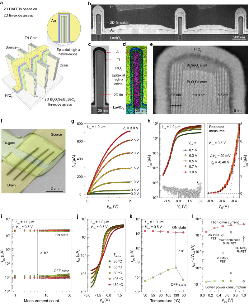
Fig. 4. Electrical performance of 2D multi-fin FinFETs based on aligned 2D Bi2O2Se-Bi2SeO5 fin-oxide arrays.
a Schematic diagram of 2D Bi2O2Se/Bi2SeO5/HfO2 FinFET with three fins. b Cross-sectional STEM image of fin arrays. c–e Low-magnification STEM image (c), Energy-dispersive X-ray spectroscopy (EDS) image (d), and high-magnification STEM image (e) of Bi2O2Se/Bi2SeO5 fin-oxide heterostructures covered with HfO2 dielectric layer. f Tilted SEM image of a 3-fin FinFET. g Typical output curves of the 2D multi-fin FET in (f). IDS is the source-drain current. VDS is the source-drain voltage and VG is the gate voltage. Lch represents the channel length of the devices. h Transfer curves of the 2D multi-fin FET in (f) and the repeated transfer curve measurement results for 50 cycles of the 2D multi-fin FET. IG is the gate leakage current, Vth is the threshold voltage and ΔVth means the shift of threshold voltage. The intersection of the two dashed lines is the threshold voltage of the device, represented by a solid line. i Statistical on-state current (ION) and off-state current (IOFF) measured over 50 cycles for different multiple-channel 2D FinFETs. j, k Transfer curves (j) and statistical ION and IOFF (k) of the 2D multi-fin FET in (f) operated under different temperatures. l Comparison of normalized current of the fabricated 2D multi-fin FETs with 2D MoS2 FET49, 2D InSe FET50, 2D MoS2 FinFETs20 and Intel’s 14 nm-node Si FinFETs51 under low gate-voltage modulation. L is the channel length and Weff is the effective width of device.

