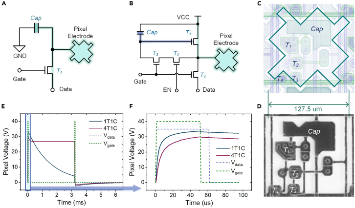
Figure 3.
FPDA pixel circuit design
(A) a 1T1C pixel circuit; (B) a 4T1C pixel circuit; (C) the layout of the 4T1C pixel circuit, (D) a photomicrograph of the 4T1C circuit; (E) pixel electrodes voltage simulation of a 1T1C and a 4T1C circuit, (F) pixel electrodes voltage charge details of the 1T1C and the 4T1C circuit.

