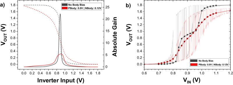
Fig. 6. Influence of the inverter’s characteristics on the p-bit output.
a Graph showing the voltage transfer curve (dotted line, left axis) and the absolute gain curve (solid line, right axis) for an untuned inverter (black) and an inverter that is tuned (red) to artificially lower the gain (by application of a body bias to the NMOS transistor in the inverter). b The averaged p-bit output, VOUT, as a function of the input voltage, VIN, for the untuned (black) and lower-gain inverter (red). Each point on the dot-line curve represents the averaged value of the p-bit’s output, obtained by fixing the input voltage (VIN) and averaging the output (VOUT) over the series of values produced due to the fluctuating MTJ resistance.

