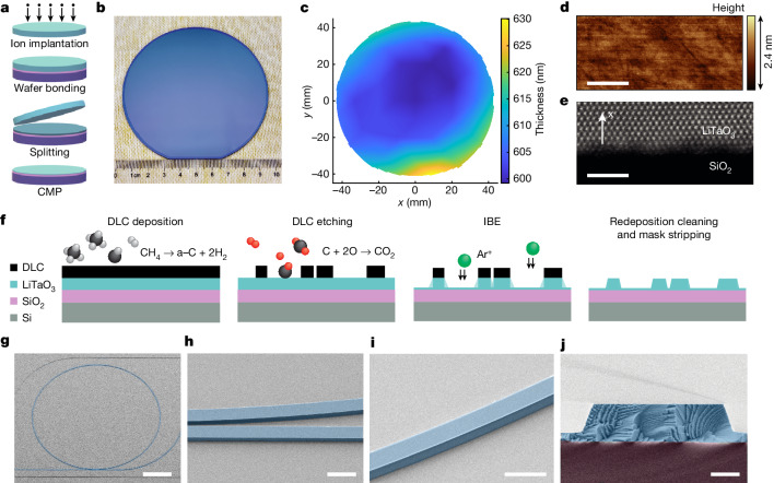
Fig. 1. LTOI substrates and optical waveguides.
a, Schematic of the LTOI wafer-bonding workflow showing hydrogen-ion implantation, bonding, splitting and chemical mechanical polishing (CMP). b, Photograph of the bonded wafer demonstrating uniform and defect-free bonding. c, Thickness map of the LiTaO3 thin film on the wafer. The x,y axes represent the distance from the wafer centre. d, Atomic force micrograph of the LiTaO3 thin film surface. Scale bar, 500 nm. e, High-resolution scanning transmission electron-microscopy image of the LiTaO3–SiO2 bonding interface. The arrow represents the x-cut crystal orientation. Scale bar, 2 nm. f, Schematic of the fabrication workflow for LTOI optical waveguides, including DLC hard-mask deposition by plasma-enhanced chemical vapour deposition (PECVD) from the methane precursor, DLC dry etching through oxygen plasma, and LiTaO3 etching by argon ion-beam etching (IBE), followed by redeposition and mask removal. The layers are DLC (black), LiTaO3 (light blue), SiO2 (purple) and Si (grey). Spheres show C (black), O (red) and Ar+ (green). g, Colourized scanning electron micrograph (SEM) of LTOI microring resonator (blue). Scale bar, 50 μm. h, Colourized SEM of etched LTOI microring and bus waveguide coupling section. Scale bar, 2 μm. i, Colourized SEM of etched LTOI waveguide and sidewall. Scale bar, 2 μm. j, Colourized SEM cross-section of etched LTOI waveguide (blue) on top of SiO2 bottom cladding (purple). Scale bar, 500 nm.

