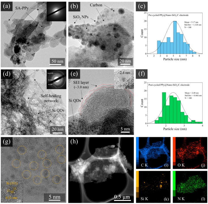
Figure 4.
TEM images corresponding SAED patterns (inset) of pre-cycled (a,b) and post-cycled (d,e) PPy@Nano-SiO2/C electrodes and particle size histograms of SiO2 NPs (c) and Si QDs (f), HRTEM image of a single Si-QDs (g) showing the (111) lattice (inset), HAADF-STEM image (h), and EDS elemental mapping images of SA-PPy@Nano-SiO2/C: overlay of C K edge (i), O K edge (j), Si K edge (k), and N K edge (l).

