Fig. 1.
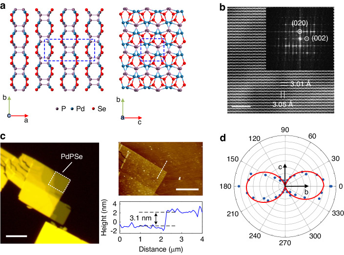
Anisotropic electron and phonon characterization of the 2D PdPSe crystal. a The lattice structure of 2D layered PdPSe with a puckered pentagonal. Left: side view of 4 L PdPSe; Right: top view of the atomic crystal structure of monolayer PdPSe. b HRTEM image of the few-layer PdPSe. Inset: the FFT pattern of Fig. 1b. Scale bar: 2 nm. c Left: The optical microscopic image of a few-layer PdPSe on the fused silica substrate. Scale bar: 5 μm; Right upper: AFM image. Scale bar: 5 μm; Right bottom: a cross-sectional profile of the edge of the PdPSe flake marked by white dashed line in the AFM image. d Polar plot of the Raman intensities for the peak as a function of the polarization angle with the parallel configuration (Fig. S3b)

