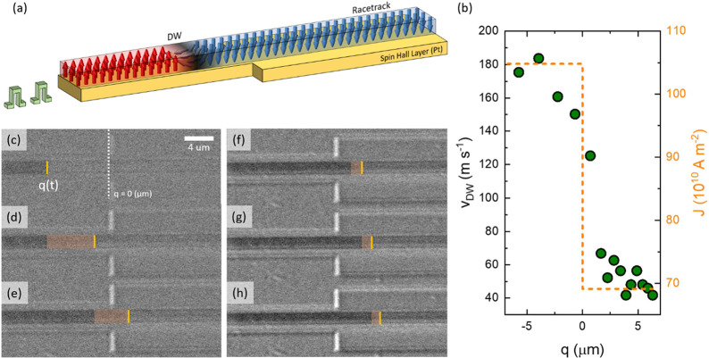
Figure 1.
(a) Schematic illustration of a passive DW controller. The device is divided into two regions so that the width of the spin Hall layer is wider in one section compared to the other, but the magnetic nanowire is uniform in width. (b) Velocity of the DW measured at various points along the nanowire. For q > 0 μm, at 11 V pulse (5 ns pulse), the current density drops (105 MA cm–2 to 69 MA cm–2) due to the increased width of the Pt layer. The drop in the current density lowers vCIDWM from ∼180 m s–1 to ∼50 m s–1. (c–h) Differential Kerr microscopy images after (c–e) injecting five consecutive pulses and (f–h) injecting 10 consecutive pulses (10 ns long, 10 V). The orange shades indicate the distance of the DW shift. Note that the speed of the DW was 88 and 36 m s–1 in section 1 (narrow region) and section 2 (wide region), respectively.

