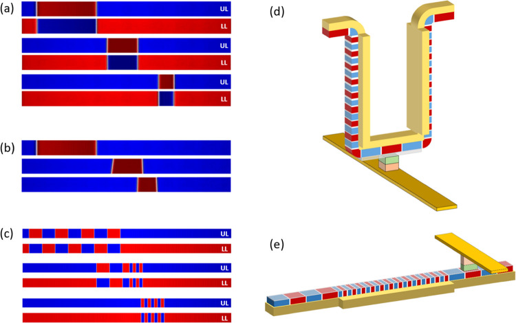
Figure 5.
Micromagnetic simulations for DW spacing control in (a) SAF and (b) FM racetracks. UL and LL denote upper and lower layers, respectively. The size of the racetrack was set to be 700 nm (length) by 50 nm (width). In the SAF, the 200 nm DW spacing shrinks to 53 nm in section 2, where the current density drops by a quarter. On the other hand, in the FM case, the 200 nm DW spacing shrinks to ∼70 nm in section 2. Note that the minimum DW spacing is larger for a FM due to the existence of the stray field. (c) Demonstration of the compression of multi-DWs in the SAF racetrack. High bit density racetrack memory device with (d) 3D and (e) linear-type structures. The extended spin Hall layer acts as a bit compressor, which can maximize the density of DW bits.

