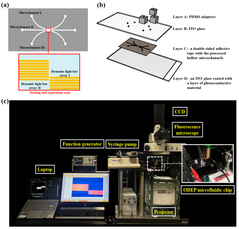
Figure 1.
(a) Layout (top-side view), (b) structure (Layers A, B, C, and D: 3 PDMS tube adapters, ITO glass, double-sided adhesive tape with processed hollow microchannels, and ITO glass coated with a layer of photoconductive material, respectively), and (c) photograph of the overall experimental setup.

