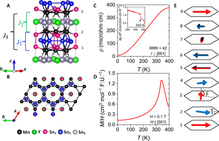
Fig. 1. Crystal structure and electrical and magnetic properties of YMn6Sn6.

(A) Sketch of the crystal structure of YMn6Sn6. (B) Top view of the structure shown in (A). Within a unit cell shown by the grey solid lines, there are two kagome planes with the formula Mn3Sn that are separated by Sn3 and YSn2 layers. The symbols Ji are the exchange constants between different Mn layers. (C) Electrical resistivity of YMn6Sn6 as a function of temperature with the electric current applied in the ab plane. Inset shows the temperature derivative of the electrical resistivity in the vicinity of TN, which shows a jump at 333 K below which an incommensurate spiral state develops. The residual resistivity ratio (RRR = ρ400K/ρ2K) is 42 indicating a good sample quality. (D) Magnetic susceptibility (M/H) of YMn6Sn6 as a function of temperature. (E) Incommensurate magnetic structure of YMn6Sn6 in the absence of external magnetic field. Arrows represent the direction of FM spins within a kagome plane. There are small constant angles α between the FM-coupled spins across the Sn3 layer, and β between the AF ones across the Sn2Y, which result in a spiral spin arrangement, where every other Mn layer forms a spiral with the pitch defined by α + β ≈ 90° and the two spirals rotated by α with respect to each other. The incommensurate spirals repeat after about four crystallographic unit cells or about nine Mn layers that are indicated by the numbers 1 to 9.
