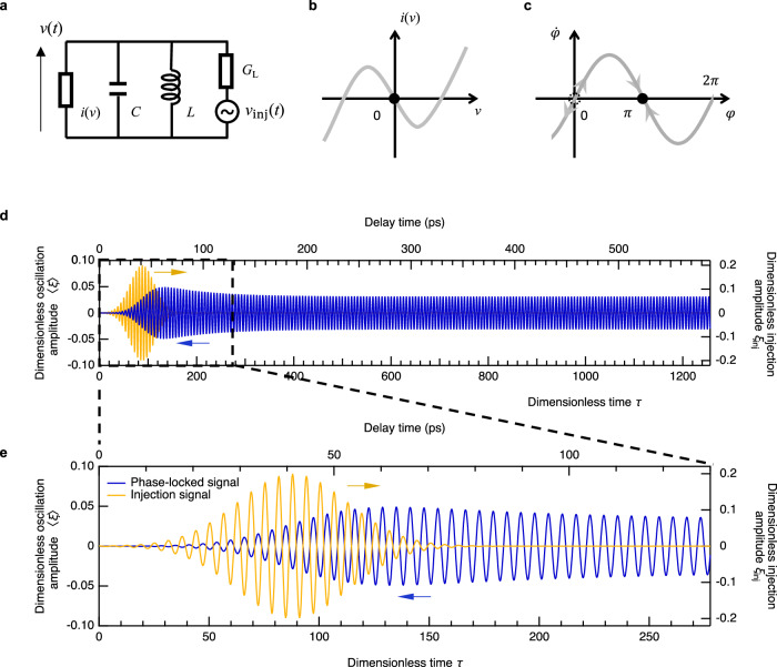
Fig. 4. Analysis based on Van der Pol model.
a Equivalent circuit. GL: load conductance, C: capacitance, L: inductance, i(v): RTD current, v(t): oscillation voltage. b. Current–voltage characteristic approximated by a cubic function. We considered the simplest case of the bias voltage at the center of the NDC region36 (inflection point), but similar results can be obtained at other bias voltages. c Phase response function of the forced Van der Pol oscillator, showing the stable steady-state solution at π. d Simulated waveform (blue, left axis) phase-locked by the injection signal (orange, right axis). e Magnified view of (d), showing the anti-phase locking behavior.

