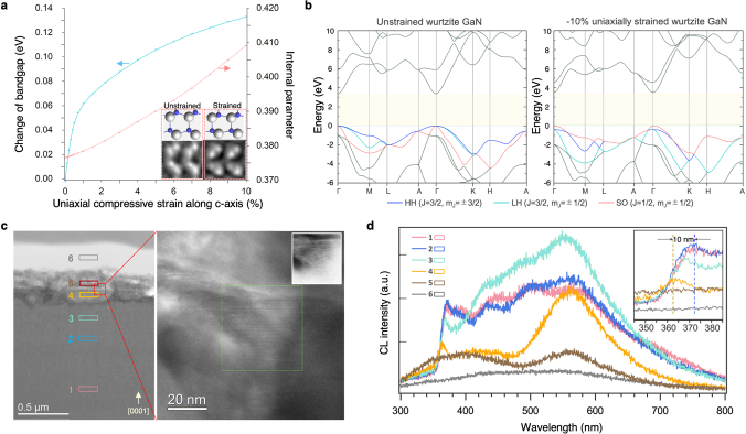
Extended Data Fig. 3. Changes in the valence band structure of strained GaN.
a, Calculated bandgap changes of wurtzite GaN and internal parameter under high uniaxial compressive strain. Insets depict schematic representations and iDPC-STEM images of unstrained GaN lattices outside the MiGs structure and strained GaN lattices within the MiGs structure. b, Calculated electronic band structures of unstrained wurtzite GaN (left) and −10% strained wurtzite GaN (right). c, STEM image of an FIB-prepared thick GaN lamella with MiGs structure distributed on the surface, where a magnified bright field (BF)-STEM image is placed on the right, with an inset showing a HAADF-STEM image of the area in the green dashed box of the BF-STEM image, confirming the presence of MiGs structures. Thicker lamella is required for STEM- cathodoluminescence (CL) analysis which compromises the STEM imaging resolution. d, STEM-CL spectra comparing photoemissions from nano-scale sampling locations far from, close to, and inside the MiGs structures formed by annealing metallic Mg deposited on an n-type GaN substrate. Positions of sampling locations are indicated in c accordingly.

